The "progress of UV light emitting core" by the R & D team of deep violet technology has been reported successively by international semiconductor authoritative journals

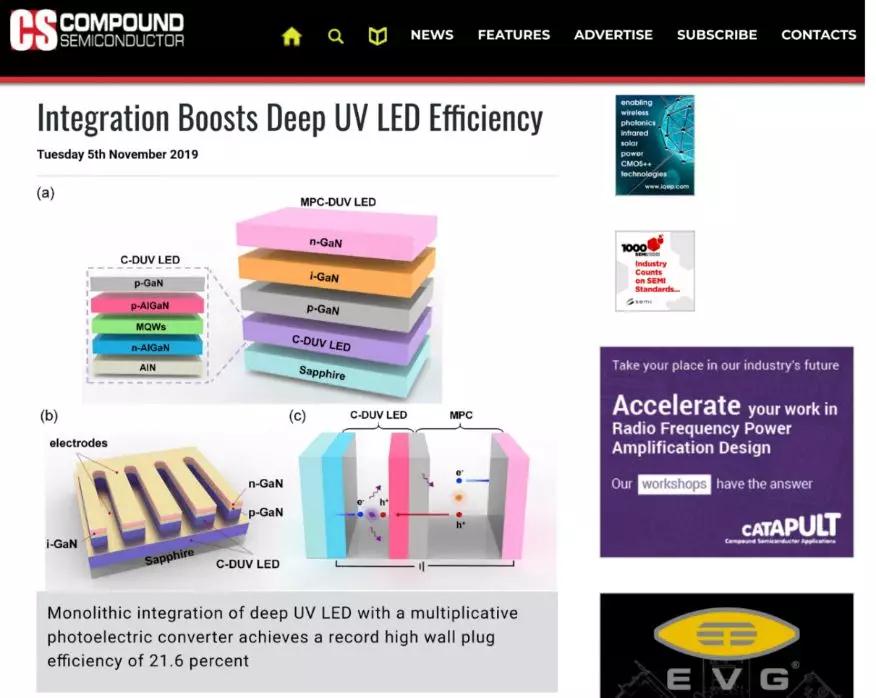
Semiconductor deep ultraviolet light emitting diode chip integrated with photomultiplier converter
The R & D team of Chen Changqing and Dai Jiangnan first integrated the p-i-n detection structure into the deep UV LED chip for the first time, realizing the carrier cycle injection, light multiplication and amplification functions, and achieved the highest electro-optic conversion efficiency of 21.6%.

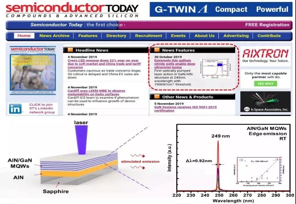
The latest deep ultraviolet laser
Chen Changqing and Dai Jiangnan research and development team first used ultra-thin AlN / GaN multiple quantum wells as the active region of deep ultraviolet laser for the first time, and realized the transverse electric mode (TE) stimulated emission phenomenon with the peak wavelength of 249 nm under room temperature optical excitation, and the threshold power density was 190kw / cm2。
For a long time, semiconductor deep ultraviolet LED technology has been widely regarded, but its photoelectric conversion efficiency has always been unable to break through 10%. It is difficult to move forward in the primary stage of commercial application. Its energy-saving, environmental protection, portability and long service life can be widely used in medical phototherapy, sterilization, air purification, secure communication, gas detection market potential can not be released.
In this regard, H. Hirayama research team of Japan Institute of physics and chemistry, and C. Kuhn research team of Berlin University of technology have put forward several ways, such as using electron barrier layer to suppress electron leakage, using tunnel junction to replace p-type aluminum gallium nitrogen layer to improve hole injection efficiency, and so on.

The research and development achievements of Chen Changqing and Dai Jiangnan solved this international problem
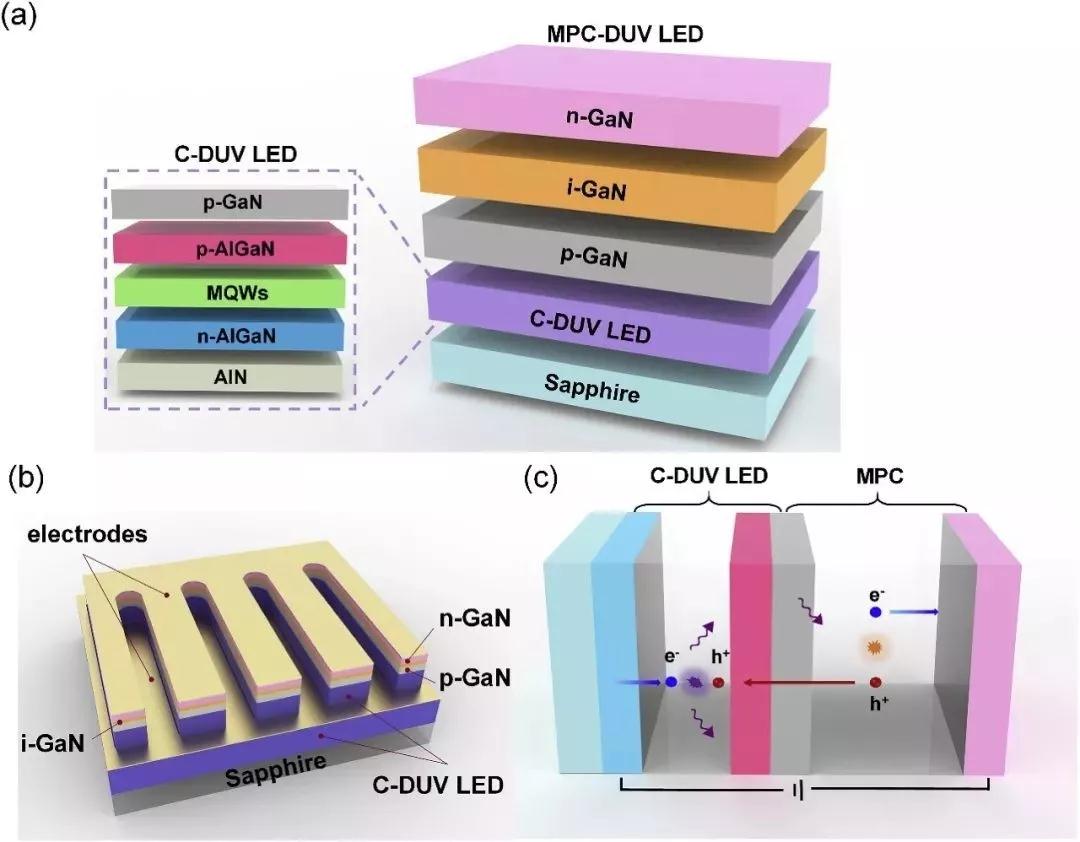
Monolithic integration technology is to integrate two or more devices or functional structures into a single chip, and improve the performance of the device by using the interaction between them. In essence, this system level innovation can build a new device environment and realize "system on chip". Chen Changqing and Dai Jiangnan research team put forward a new idea of introducing monolithic integration technology. The p-i-n Gan detection structure was grown on the deep ultraviolet LED epitaxial structure (mpc-duv LED) in situ to realize the chip device with carrier cycle injection and photomultiplier amplification.
Through a long period of research and exploration, the team of Chen Changqing and Dai Jiangnan creatively applied the p-i-n detection structure in the deep ultraviolet LED chip, which can absorb the deep ultraviolet light below 280 nm emitted by the active region of the quantum well, and convert it into a new electron hole pair. Under the action of high voltage, the generated electron hole pairs are separated, and the hole carriers drift in the direction of the vector well under the action of electric field, and then re injected into the quantum well.

It is found that under low current, the traditional DUV LED chip is driven by current, and its output power increases linearly. In contrast, mpc-duv LED chip is voltage driven, and its output power increases exponentially.
The real power of point a is 33.0 μ W. For the traditional DUV led, the operating voltage and current are 4.88 V and 1.87 Ma respectively, while for mpc-duv led, the operating voltage and current are 19.5 V and 7.85 μ a, respectively. The electro-optic conversion efficiency (output power / injected power) of the two DUV LED are 0.36% and 21.6%, respectively, with a difference of 60 times.

The research further reveals the mechanism of ultra-high conversion efficiency of mpc-duv LED chip under low current. Through APSYS simulation, the electric field in i-gan layer can reach 5 × 10⁶V / Therefore, there is a great probability that collision ionization will occur in the depletion layer, and a high gain of tens or even hundreds of times will be obtained, thus increasing the order of magnitude of hole carriers.6 V/cm, therefore there is a high probability of collision ionization occurring in the depletion layer, achieving high gain of tens or even hundreds of times, thereby achieving an increase in the number of hole carriers.
In the whole process of the photoelectric cycle, the electrons and holes in the quantum well emit compound luminescence, some of the deep ultraviolet photons escape from the bottom of the device, and the other photons enter the MPC structure to be absorbed. The high-energy deep ultraviolet photons excite gallium nitride to produce corresponding electron hole pairs, and separate under the applied voltage. The holes are under the strong electric field in the depletion region In this way, the carrier injection efficiency is greatly improved.
UV in the refrigerator can play a role in sterilization
Technology sharing · November 15, 2017 · 937 views
Comparison of driving circuits for deep UV uvc-led
Technical sharing · July 3, 2019 · 2678 views
How to evaluate the sterilization effect of UV LED
Technology sharing · February 28, 2020 · 1838 views
Topic sharing: deep UV uvc-led
Technology sharing · February 20, 2020 · 1197 views
Development of deep UV LED
Technology sharing · December 6, 2020 · 1330 views
Water related approval approved, and Youweixin has obtained authoritative certification in the field of drinking water hygiene and safety
Company News, September 24th, viewed 97 times
Warmly welcome Professor Sun Xiaowei, Professor Sun Haiding, Associate Professor Wang Kai and their delegation to visit Shenzhen purple science and technology investigation and handover
Company News, November 18, 2018, viewed 797 times
Looking forward to a new starting point and fighting for a new stage
Company News, January 31, 2021, viewed 369 times
